nextnano3 - Tutorial
next generation 3D nano device simulator
1D Tutorial
Dispersion in infinite superlattices: Minibands (Kronig-Penney model)
Author:
Stefan Birner
-> 1Dsuperlattice_dispersion_4nm_nn3.in
/ *_nnp.in -
input file for the nextnano3
and nextnano++ software
-> 1Dsuperlattice_dispersion_6nm_nn3.in       /
*_nnp.in -
-> 1Dsuperlattice_dispersion_bulk_GaAs_nn3.in / *_nnp.in -
-> Superlattice_1D_nn3.in
/ *_nnp.in
-
These input files are included in the latest version.
Dispersion in infinite superlattices: Minibands (Kronig-Penney model)
This tutorial aims to reproduce two figures (Figs. 2.27, 2.28, p. 56f) of
Paul Harrison's
excellent book "Quantum
Wells, Wires and Dots", thus the following description is based on the
explanations made therein.
We are grateful that the book comes along with a CD so that we were able to
look up the relevant material parameters and to check the results for
consistency.
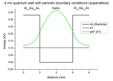
Superlattice 1: 4 nm AlGaAs / 4 nm GaAs
- Our infinite superlattice consists of a 4 nm GaAs quantum well
surrounded by 2 nm Al0.4Ga0.6As barriers on each side.
The choice of periodic boundary conditions leads to the following sequence of
identical quantum wells: 4 nm AlGaAs / 4 nm GaAs / 4 nm AlGaAs / 4 nm GaAs /
... . So our superlattice period has the length L=8 nm.
(Actually it has the length L = 8.25 due to the grid point resolution of 0.25
nm.)
This figure shows the conduction band edge and the first eigenstate that is
confined inside the well and its corresponding charge density (psi²) for
the superlattice vector kz = 0. Note
that periodic boundary conditions are employed for solving the Schrödinger
equation. The second eigenstate is not confined inside the well and is
therefore not shown here.
(Note that the energies were shifted so that the conduction band edge of GaAs
equals 0 eV.)
- In a superlattice the electrons (and holes) see a periodic potential which
is similar to the periodic potential in bulk crystals. This means that the
particle wave functions are no longer localized in one quantum well. They
extend to infinity and they are equally likely to be found in any of
the quantum wells. The eigenstates are called Bloch states (as in bulk)
and the wave functions are periodic:
Psi (z) = Psi (z + L)
For a travelling wave of the form exp(ikzz) it holds:
Psi (z + L) = exp(ikz(z + L)) = exp(ikzz) exp(ikzL)
i.e. Psi (z + L) = Psi (z)
exp(ikzL)
kz is the momentum of the electron (or hole) along the growth
direction of the infinite superlattice.
- Here we plot the superlattice dispersion curve, i.e. the energy of the
electron as a function of its superlattice wave vector kz for the
lowest eigenstate. As the energy is a periodic function of kz with
period 2pi/L, we plot only the interval [ - pi / L , + pi / L].
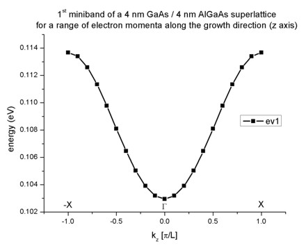
The plot is in excellent agreement with Fig. 2.27 (page 56) of
Paul Harrison's
book "Quantum
Wells, Wires and Dots".
When the electron is at rest (kz=0), the dispersion curve shows a
minimum. As the electron momentum kz increases, its energy also
increases and reaches a maximum at k = - pi/L and k = + pi/L. Thus the
electron within the superlattice occupies a continuum of energies. This
continuum that is bound by a maximum and a minimum of energy is called
miniband. Due to the similarity with the energy bands of a bulk crystal,
the point in the superlattice Brillouin zone for kz=0 is
called Gamma and for kz=pi/L it is called X.
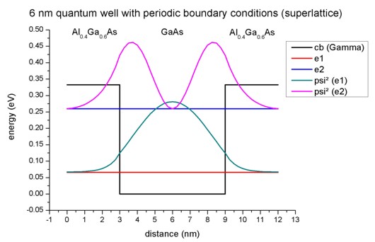
Superlattice 2: 6 nm AlGaAs / 6 nm GaAs
- Our second infinite superlattice consists of a 6 nm GaAs quantum
well surrounded by 3 nm Al0.4Ga0.6As barriers on each
side. The choice of periodic boundary conditions leads to the following
sequence of identical quantum wells: 6 nm AlGaAs / 6 nm GaAs / 6 nm AlGaAs / 6
nm GaAs / ... . So our superlattice period has the length L=12 nm.
(Actually it has the length L = 12.25 due to the grid point resolution of 0.25
nm.)
This figure shows the conduction band edge and the two lowest eigenstates that
are confined inside the well and their corresponding charge density (psi²)
for the superlattice vector kz = 0.
Note that periodic boundary conditions are employed for solving the
Schrödinger equation. The third eigenstate is not confined inside the well and
is therefore not shown here.
In contrast to the 4 nm quantum well superlattice described above, two
confined electron states exist.
(Note that the energies were shifted so that the conduction band edge of GaAs
equals 0 eV.)
- The following figure shows the first two minibands for this superlattice.
They arise from the first and the second eigenstate. Note that due to the
scale of this figure the first miniband looks almost flat. It is also
interesting that for the second miniband the minimum is not at the center
(i.e. at Gamma) but at the edges of the superlattice Brillouin zone at X (and
-X).
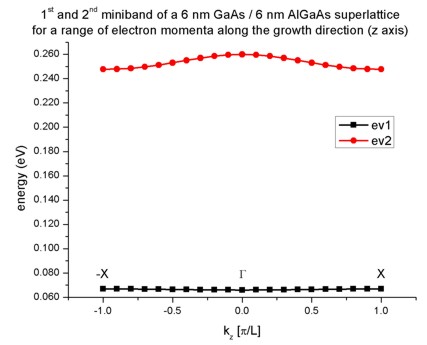
Again, the plot is in excellent agreement with Fig. 2.28 (page 57) of
Paul Harrison's
book "Quantum
Wells, Wires and Dots". However, the caption of Fig. 2.28 incorrectly
states that this should be a 8 nm GaAs / 8 nm Al0.4Ga0.6As
superlattice. In fact, it must be a 6 nm GaAs / 6 nm Al0.4Ga0.6As
superlattice.
Technical details
- The resolution of the miniband plot has to be specified within the keyword
$quantum-model-electrons:
$quantum-model-electrons
  ...

  boundary-condition-001 = periodic !
periodic boundary conditions are necessary for superlattices
  num-ks-001
  = 21       !
The miniband dispersion is written to this file:
Schroedinger_1band/sg_dispSL1D_el_qc001_sg001_deg001_evmin001_evmax002.dat
It contains the following data:
  k_z [pi/L]        k_z [1/AA]
  1st eigenvalue      2nd
  eigenvalue

  -1.0
  ...
  ...
  ...
Dispersion in bulk GaAs with periodic boundary conditions
We take the same input file as 1Dsuperlattice_dispersion_6nm_nn3.in
but this time we replace the AlGaAs barrier with GaAs so that we have
only pure bulk GaAs with a length of 12 nm. So our superlattice period has the
length L=12 nm.
(Actually it has the length L = 12.25 due to the grid point resolution of 0.25
nm.)
At the boundaries we apply periodic boundary conditions and the same
superlattice options as above:
1Dsuperlattice_dispersion_bulk_GaAs_nn3.in:
$quantum-model-electrons
  ...

  boundary-condition-001 = periodic !
periodic boundary conditions are necessary for superlattices
  num-ks-001
  = 21       !
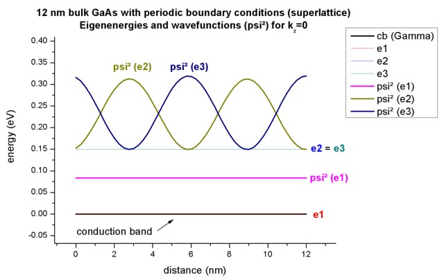
This figure shows the conduction band edge and the three lowest eigenstates and their corresponding charge density (psi²)
for the superlattice vector kz = 0.
Note that periodic boundary conditions are employed for solving the
Schrödinger equation.
- The ground state wave function is constant with its energy equal to the
conduction band edge energy.
- The energies of the second and third eigenstate are degenerate.
(Note that the energies were shifted so that the conduction band edge of GaAs
equals 0 eV.)
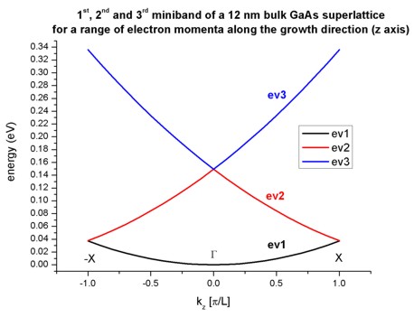
The following figure shows the first three minibands for this superlattice.
They arise from the first, second and third eigenstate.
The second and third eigenstate are degenerate at kz = 0 as can be
seen also in the figure above. Also at kz = -1 and kz = 1,
the first and second eigenstate are degenerate. This is as expected because the
dispersion should look like the parabolic dispersion E(k) of bulk GaAs.
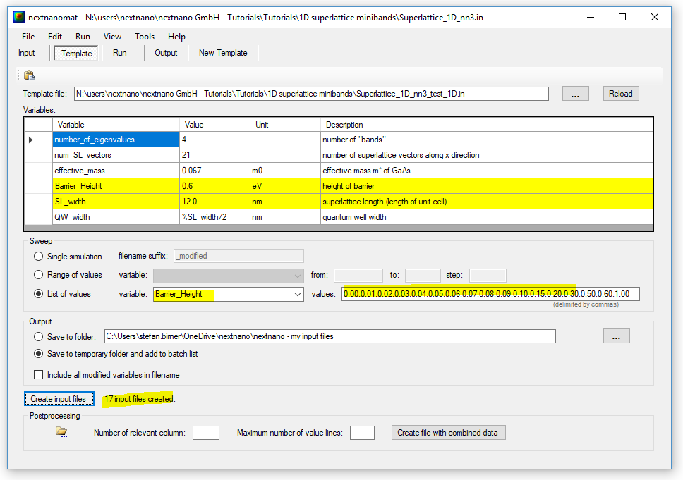
Template
-> Superlattice_1D_nn3.in
/ *_nnp.in
-
input file for the nextnano3
software
We want to study the energy levels of a superlattice in order to understand how they
form bands in a periodic structure.
One can easily see this by calculating the energy levels for various barrier
heights, i.e. we automatically generate input files for the variable
"Barrier_Height".
Once done, we visualize the "band structure file" called
sg_dispSL_el_sg1_deg1_piL_evmin001_evmax004.dat.
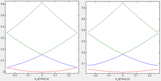
The left figure contains a quantum well superlattice with a barrier height of 0
eV, i.e. a bulk semiconductor while the figure on the right shows the dispersion
for a barrier height of 0.06 eV.
One can clearly see that three energy band gaps open.
|